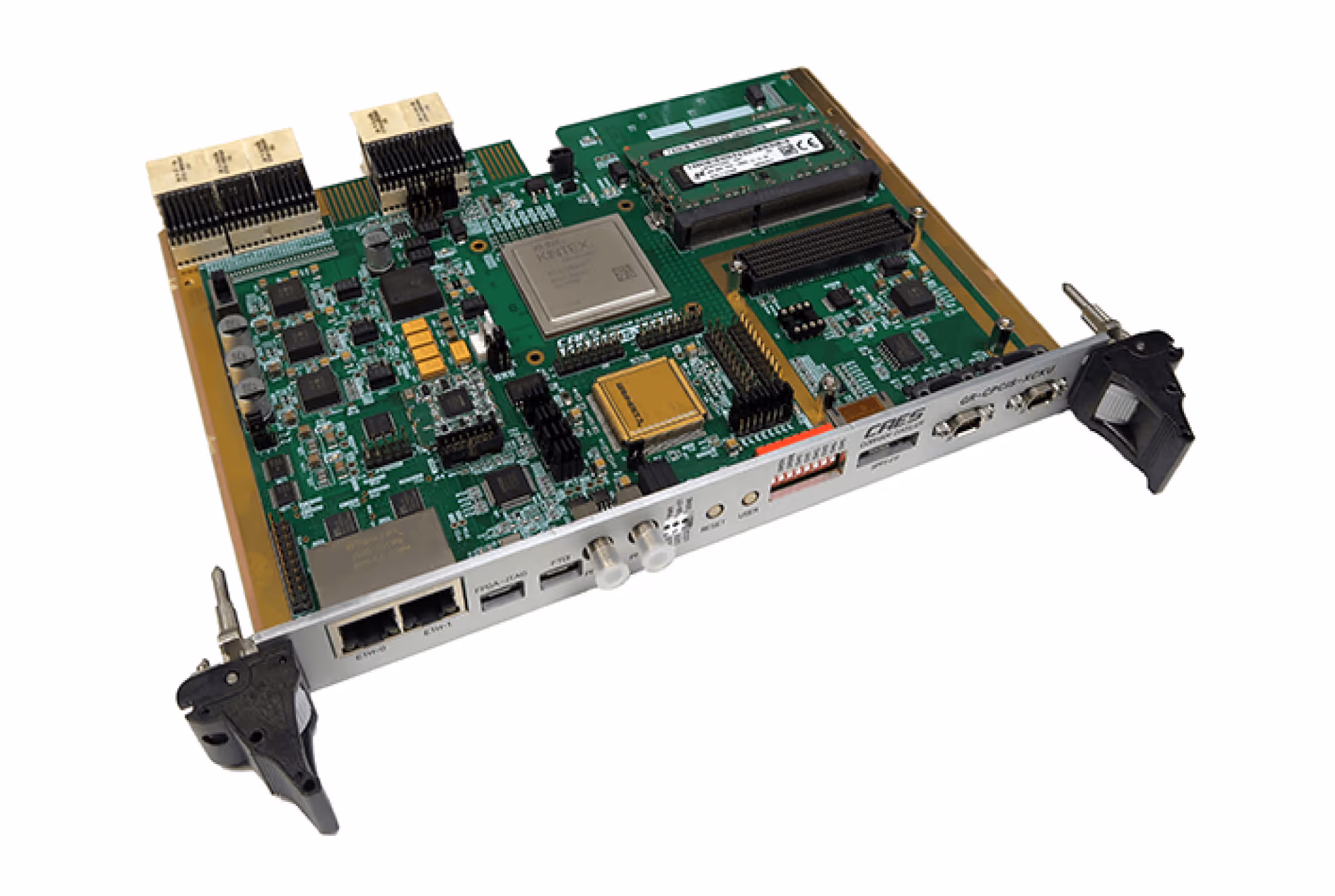
GR-CPCIS-XCKU

The GR-CPCIS-XCKU is a 1 slot, 6U high board with a CPCI-S backplane format, and can be used stand alone on the bench top, or installed in a CPCI-Serial rack.
The SRAM-based FPGA on the board is susceptible to single event upsets (bit flips) in its configuration memory when used in harsh environments. 

Protecting the design implemented in the FPGA fabric against these radiation effects requires scrubbing the FPGA configuration memory to prevent accumulation of errors. This is done through the inclusion of the radiation hardened GR716 microcontroller on the FPGA board. The microcontroller acts as a supervisor to the FPGA and can prevent accumulation of errors. The GR-CPCIS-XCKU has commercial and prototype grade components and is not suitable for operation in a space environment. The board is intended as a prototype platform for development


GR-CPCIS-XCKU

FPGA

The board implements a large Xilinx Ultrascale FPGA, in a XCKU060 sized device 1517 ball-grid-array package and is compatible with larger devices of the same series which have the same footprint (See table below). The GR-CPCIS-XCKU board features an optional GR716 microcontroller acting as a supervisor for the FPGA.

   
FPGA  XCKU060 
XCKU115

LUTs (K)

726

1451

DSP slices

2760

5520

BRAMs (Mb)

38

75.9

The FPGA development board has the following features: 

  • Xilinx XCKU, in 1517 pin FCBGA package.
  • GR716 microcontroller - Optional
  • FPGA interface to DDR3 SDRAM via two SODIMM connectors.
    • 64-bit data bus on first SODIMM. Up to 4GiB.
    • 32-bit data bus on second SODIMM. Up to 2GiB.
  • SPI flash for FPGA configuration (512 Mbit), for GR716 boot (256 Mbit), and for data (256 Mbit). The FPGA has also access to two NVM: 512 Mbit SPI and Parallel Flash memory (40 bit wide)
  • Power, Reset, Clock and Auxiliary circuits.
  • FMC Mezzanine expansion connector.
  • Scrubbing interface for FPGA. Available also without the GR716. 
  • A 2×10 connector to interface with a GR-ACC-6U_6UART breakout board providing access to 6 UARTS (or 16 GPIOs).
  • The backplane interfaces of the board are:
    • 8 x SpaceFibre for full-mesh interconnect using FPGA GTH banks
    • 8 x SpaceWire for dual-star interconnect
    • Dual-redundant CAN-bus to FPGA and/or GR716 via two or four transceivers
    • SGPIO and I2C connected to FPGA with jumper-configurable pull-ups
    • 12V supply from backplane that can be turned off by the external input PS_ON#
    • Other utility signals connected to the FPGA
  • The front-panel interfaces are:
    • JTAG access to FPGA and FMC (separate chains)
    • GR716 debug UART and two FPGA UARTs
    • 2x RJ45 to FPGA via magnetics and Gbit Ethernet transceivers. RGMII interface to FPGA
    • 1x eSATA for SpaceFibre to FPGA via CML redriver.
    • 2x MDM9 for SpaceWire via LVDS transceivers/repeaters to FPGA.
    • Status LEDs, push-buttons and switches
    • 2xSMA or 2xSMB for PPS time distribution to FPGA.
    • 2xUSB ports for
  • 6U high, 1 slot wide module for mounting in the controller slot of a 6U rack with a CPCI-S Space Backplane.
  • The dimensions of the main PCB are 233.35x160mm (excluding the connector protrusions).


Documentation

Document File
GR-CPCIS-XCKU Datasheet and User's Manual

GR-CPCIS-XCKU-DSUM.pdf (Nov 2023)


Development Kit Contents

Development Board:
  • GR-CPCIS-XCKU Development Board
Cable Set:
  • Laboratory power cable (Banana-to-MOLEX-2pin)
  • FPGA Heat Sink + Fan assembly (12V)
  • DDR3-SODIMM Modules (2x)