NAND Flash Memory Controller with DMA

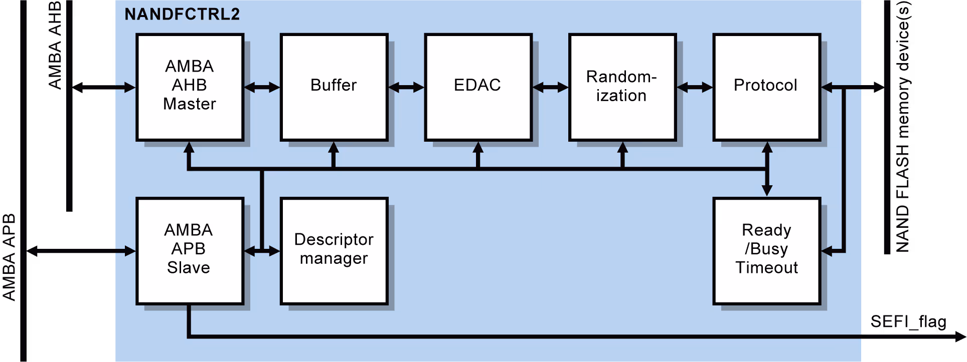
NANDFCTRL2 is a VHDL IP core implementing an interface to NAND flash memory devices. The memory controller is designed to operate with ONFI 4.0 flash memory devices and provides DMA transfers to and from the memory. The core implements a BCH EDAC with the capability of correcting 60 errors per chunk of 1024 bytes of data. The actual error correction capability is configured by means of VHDL generics, in conjunction with the configuration of memory support. The EDAC can be combined with a data randomizer, which breaks any repetitive bit patterns, thereby increasing memory endurance. Both the EDAC and the Randomizer can be bypassed during runtime if the user needs to access the memory without them.


To support detection and recovery from SEFI, the core provides timeout functions in addition to the EDAC. The SEFI detection functionality monitors ongoing accesses towards the flash to detect if any access is too long, which could indicate an error in the memory.

NANDFCTRL2 can optionally be implemented without an EDAC and have the functionality implemented in software in order to save hardware resources when targeting smaller devices.

For details about the actual flash memory interface, flash memory architecture and ONFI 4.0 command set please refer to the Open NAND Flash Interface specification, revision 4.0.


The NAND Flash controller has the following features:
  • ONFI 4.0 support
    • All mandatory ONFI 4.0 commands
    • Asynchronous / SDR data interface timing mode 0-5
  • BCH EDAC with up to 60 bits correction capacity per 1024 bytes chunks of data
  • Randomization of memory data
  • Basic timeout-based SEFI detection and reporting
  • 8-bit data interface with support for up to 64 targets and 16 channels (16x 8 bits data channels)
  • Support for up to 64 targets and 16 channels (16x 8 bits data channels)
 

Targets

The memory controller has been tested with the UT81NDQ512G8T, the 69F256G16, and the 3DFN128G08US8761 NAND flash memories.

Availability

NANDFCTRL2 is part of the GRLIB IP Library from April 2022 and can be licensed as a separate add-on. The current version of the core is suitable for users that want to include NANDFCTRL2 in products and is suitable for both ASIC and FPGA implementations. Additional features for the NANDFCTRL2 IP core will become available as part of milestone releases. The table below shows the planned milestones. Please note that the future milestone features and dates are tentative. Please click this link to sign up to receive notifications about product and documentation updates.


Milestone Description Target users Date
Release 2.0 Release 2.0 adds the features listed below:
  • Command support. Additional optional ONFI commands and vendor-specific commands
  • Improved performance and scalability including integrated multi-plane support
  • All timing modes including EDO in SDR
  • Feature to read flash memory soft bits to enable a software LDPC implementation.
  • FT features.
  • ASIC implementation support.
Users that want to include NAND flash memories in products. Suitable for both ASIC and FPGA implementation. Available
Release 2.5 Release 2.5 adds support for implementing NANDFCTRL2 with NV-DDR2 and NV-DDR3 support on Microchip and Xilinx FPGAs.
  • Synchronous interfaces: NV-DDR2 and NV-DDR3 targeting technology-specific PHY. Note: The controller depends on 3rd party PHY to support NV-DDRx.
  • Timing mode 0-9 in NV-DDR2 and NV-DDR3.
  • Example NV-DDR2 PHY targeting are Xilinx Kintex Ultrascale and Microchip PolarFire
  • Example NV-DDR3 PHY targeting Xilinx Versal FPGA.
  • ASIC implementation support.
Users that want to include NAND flash memories in products. Suitable for both ASIC and FPGA implementation. Capable for SLC-based flight grade Raw NAND Flash interfaces, with the exception of flight assurance related to FPGA PHY implementations. 2023-Dec
Future implementations Future implementations are pending customer demands and include:
  • Synchronous interface NV-DDR
  • Example NV-DDR, NV-DDR2 and NV-DDR3 PHY for additional FPGA platforms including Microchip RTG4
  • Hardware LDPC ECC for supporting MLC and TLC modes.
Users that want to include NAND flash memories in products. Suitable for both ASIC and FPGA implementation. Pending customer demand


LEON3-XCKU-NANDFCTRL2-EX Example Design

The LEON3-XCKU-NANDFCTRL2-EX is an example bitstream for the Xilinx KCU105 Evaluation Kit interfacing with the Frontgrade UT81NDQ512G8T mezzanine board.

To get access to the evaluation bitstream, contact sales@gaisler.com.

Contact your local Frontgrade representative to get access to the UT81NDQ512G8T mezzanine board.


Documentation 

 Document  File
NANDFCTRL2 IP Core User's Manual

 grip.pdf (See section NANDFCTRL2)

NANDFCTRL2 FPGA Resources Utilization

 grlib_area.xls (See NANDFCTRL2-EX sheet)

LEON3-XCKU-NANDFCTRL2 Example Bitstream User's Manual

 LEON3-XCKU-NANDFCTRL2-EX-UM.pdf

LEON3-XCKU-NANDFCTRL2 Example Bitstream Quick Start Guide

 LEON3-XCKU-NANDFCTRL2-EX-QSG.pdf