.avif)
Silicon IP
With decades of heritage and proven success in countless missions, the LEON family continues to set the benchmark for excellence in space technology.
Providing the computational power needed for satellite control, data processing, and communication systems.
Ensuring reliable performance for space exploration instruments and experiments.
Extending space-grade reliability to critical ground-based applications such as industrial control and safety systems.

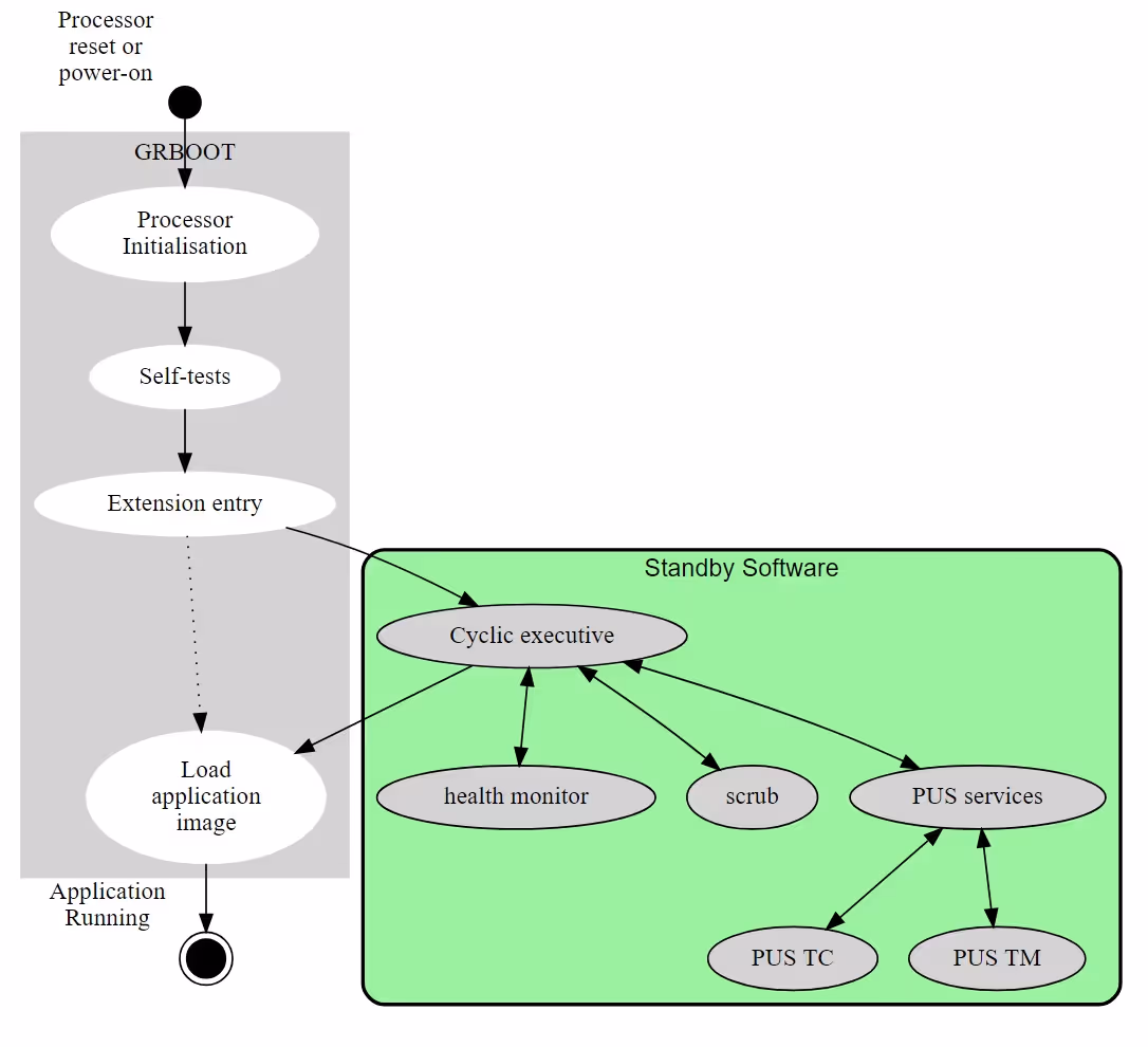
The LEON processors are fully compliant with the SPARC V8 architecture and are supported by a well-established development ecosystem, especially for space applications.

Engineered with the harsh conditions of space in mind, our processor cores offer fault tolerance features that ensure reliable operation in extreme environments.

With a range of performance options, the LEON line provides efficient solutions for both low-power embedded systems and high-performance applications.

Our LEON IP Core Processors are designed in VHDL and target FPGA and ASIC designs. They enable the creation of FPGA designs in various technologies (e.g., AMD/Xilinx, Intel/Altera, Lattice, Microchip, and NanoXplore) and are easily portable between different nodes.

The LEON processors are integrated with a rich set of IP cores from the GRLIB IP library, simplifying the development of complex systems-on-chip (SoCs) and reducing time-to-market.

With a legacy of successful missions, the LEON processors are trusted by space agencies and aerospace companies worldwide for their reliability and performance.

Our dedicated team of experts provides extensive support and resources to ensure you maximize the potential of LEON processors.


DDR2/DDR3 SDRAM, 32-bit PC133 SDRAM, SRAM, QSPI, NAND flash, parallel PROM

SpaceWire interface and router, SpaceFibre and WizardLink controller, 32-bit PCI bridge, CCSDS/ECSS Data Handling, 10/100/1000 Mbit Ethernet MAC, USB 2.0 host and device controllers, SelectMap FPGA Supervisor, CAN FD, MIL-STD-1553B, SPI, I2C, UART

AHB and APB controllers, AHB to AHB bridge, AHB to AXI bridge, L2 Cache, FPUs


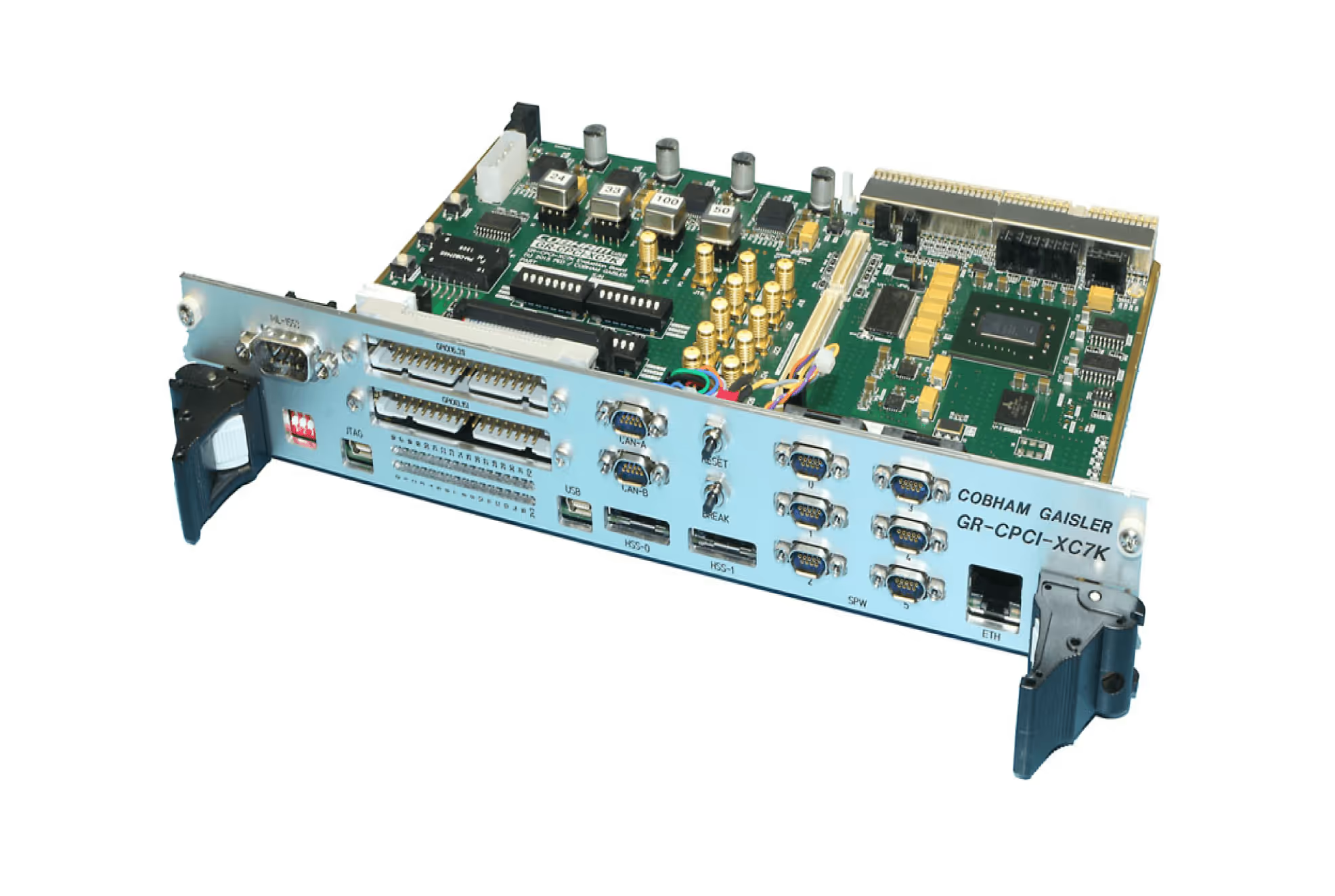
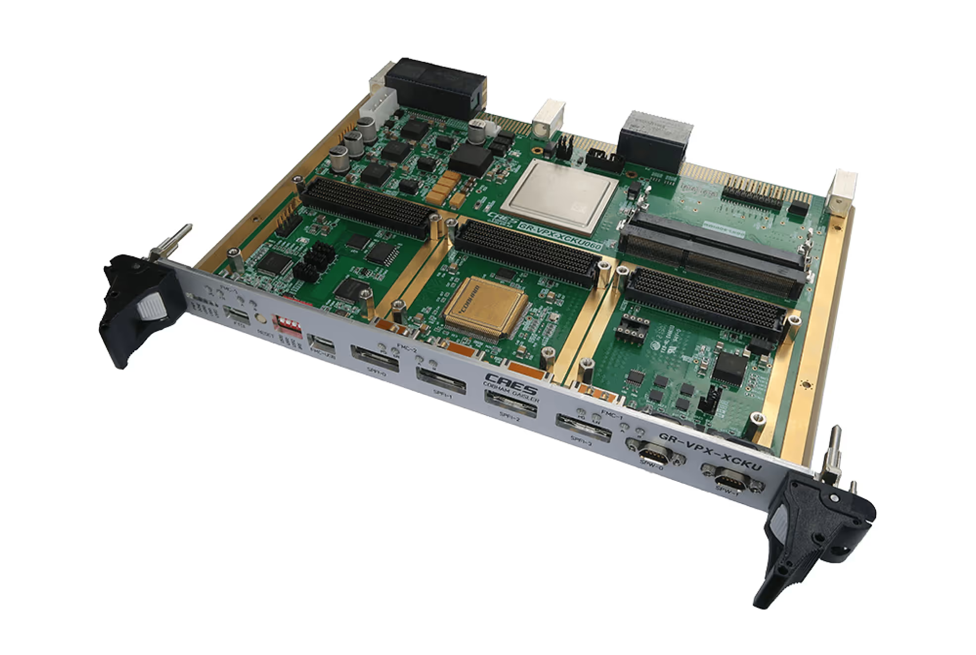
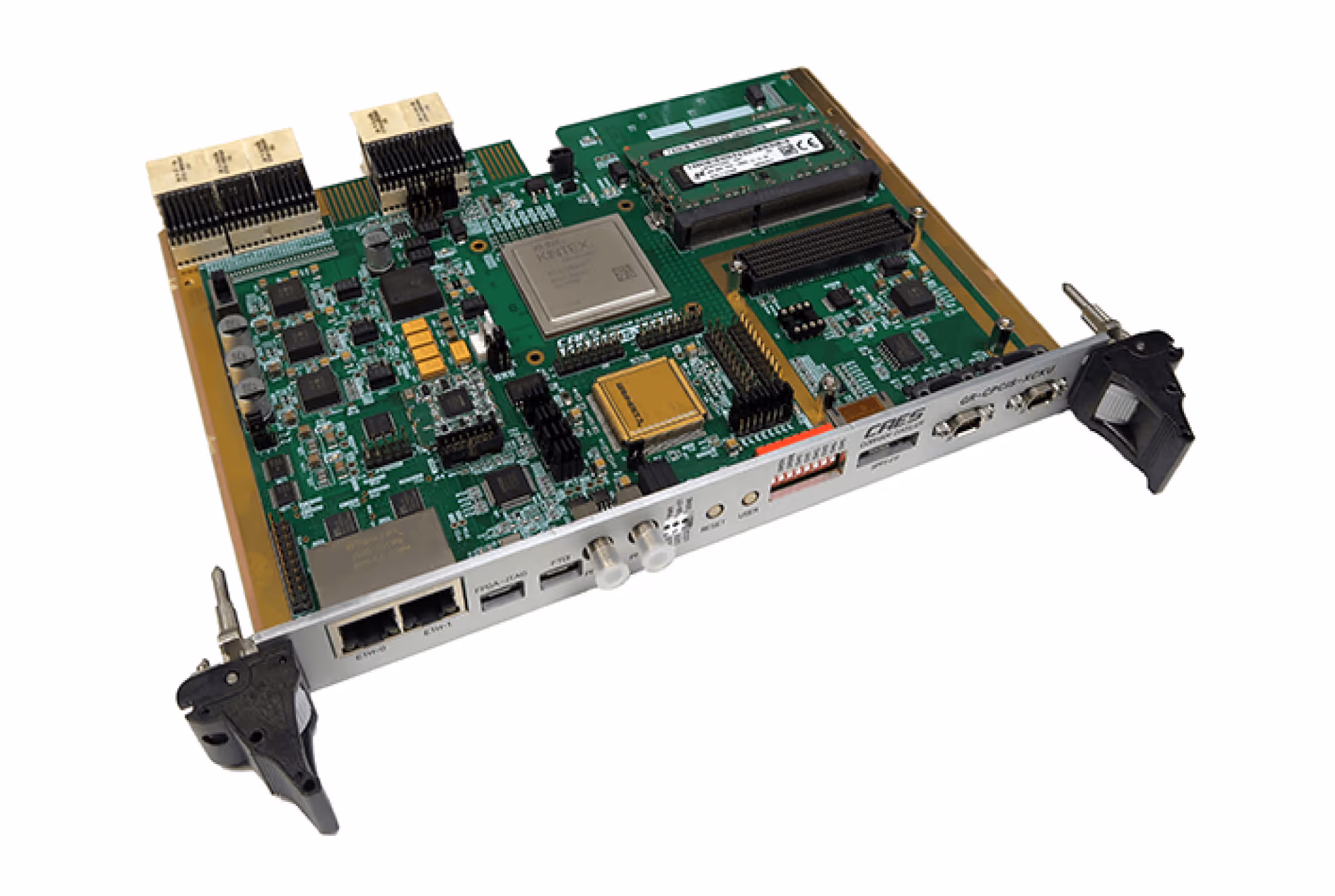
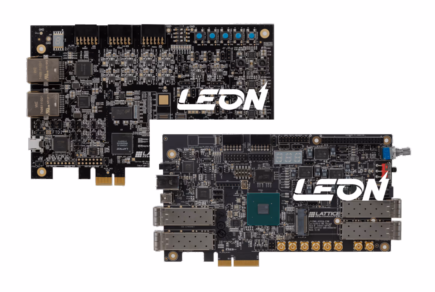
To allow users to quickly get started with their development, GRLIB contains template designs for common commercial FPGA evaluation boards. Template designs for SoC development contain commonly used IP cores such as processors, memory controllers and communication interfaces tailored for specific development boards and with targeted constraints. They provide a reliable starting point for customization and optimization, enabling designers to concentrate on the unique aspects of their SoC design.A list of the supported FPGA evaluation boards is available in the GRLIB IP Library User's Manual.We also provide evaluation bitstreams for our processors. See LEON examples and NOEL-V examples
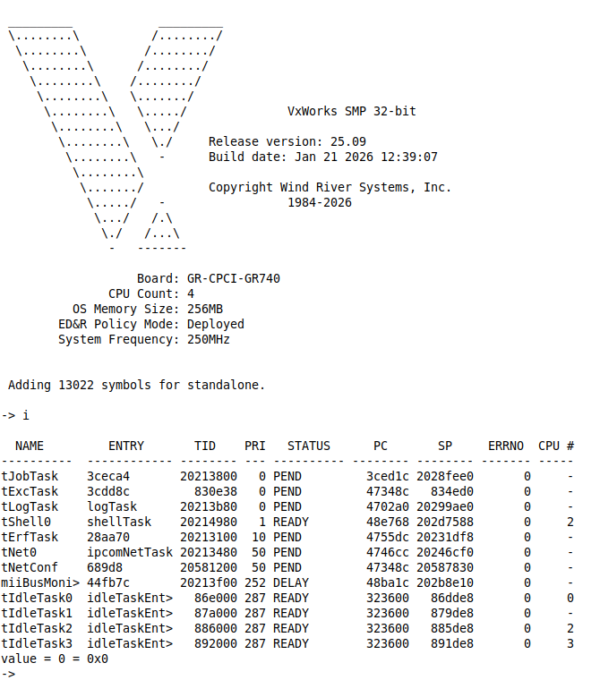
The GRMON3 hardware debugger enables developers to efficiently diagnose and resolve issues. With drivers that simplify the control of processors and peripherals, GRMON3 provides a powerful tool for troubleshooting complex systems. The debugger has the ability to connect to the SoC through various types of communication interfaces for monitoring and testing purposes. This allows developers to debug their systems at all stages of the design process, from the early stages of hardware bring-up to the final stages of software development.
The GRLIB community is a discussion platform that can be used by open-source users of the library to seek help, share information, discuss, and collaborate. See https://grlib.community GRLIB commercial users can benefit from an optional support agreement that provides them with direct communication with the development team.
The GRLIB IP Library is available in both open-source and commercial versions. The open source IP cores are distributed under the GNU GPLv2 license, making it ideal for academic purposes, evaluation, and prototyping. However, the GPLv2 license poses restrictions on commercial products, so GRLIB presents a commercial licensing option for those who require proprietary designs. The commercial distributions provide access to additional IPs and target technologies not included in the open-source version. The GRLIB IP Core User's Manual provides a complete list of all IP cores, along with information about which GRLIB distribution(s) includes each IP core. We also have a collection of FAQs on the licensing topic.

DEVICE
GR716A
GR716B
Max Frequency
50 MHz
100 MHz
On-Chip RAM
192 KiB
192 KiB
Support for single 3.3V supply
Yes
TBD
Processor
LEON3FT
LEON3FT
Real-Time Accelerator (RTA)
No
Yes, 2x
Off-chip Memory
PROM/SRAM/SPI/I2C with EDAC
PROM/SRAM/SPI with EDAC
SpaceWire
2x Endpoints
Router (2x external, 1x internal ports)
MIL-STD-1553
Yes
Yes
CAN
2x CAN 2.0 controllers
1x CAN-FD controller
PacketWire with CRC
Yes
Yes
I2C
Yes
Yes
FPGA supervisor
No
Yes
Ethernet
No
10/100 Mbit/s
ADC
2x 11bits resolution @ 200ksps8 differential/16 single-ended channels
4x ADC 11bits/14bits @ 500Ksps8 differential/16 single-ended channels
DAC
12bit @ 3Msps, 4 channels
12bit @ 3Msps analog DAC, 4 channels
Fast analogue comparators
No
20x
PWM-DAC
No
Yes, 8x
Availability
Flight models available
Prototypes in 2024
Product
GR765
GR740
GR712RC
Status
In development
TRL 9
TRL 9
Number of Cores
8
4
2
Operating frequency
1 GHz
250 MHz
100 MHz
DMIPS/Core, total
3.25k,26k
425, 1700
140, 280
Total Ionizing Dose krad (Si)
TBD
300
300
SEL Immunity (MeV-cm^2/mg)
TBD
> 125
> 118
Package
Plastic
Ceramic or plastic
Ceramic
Reach out to explore how our technology can accelerate your innovation and development projects
Learn about how we advance technology and push boundaries, everyday
Get in touch with us by submitting the form or contacting us at sales@gaisler.com
Do you have a support request or need help?
Support
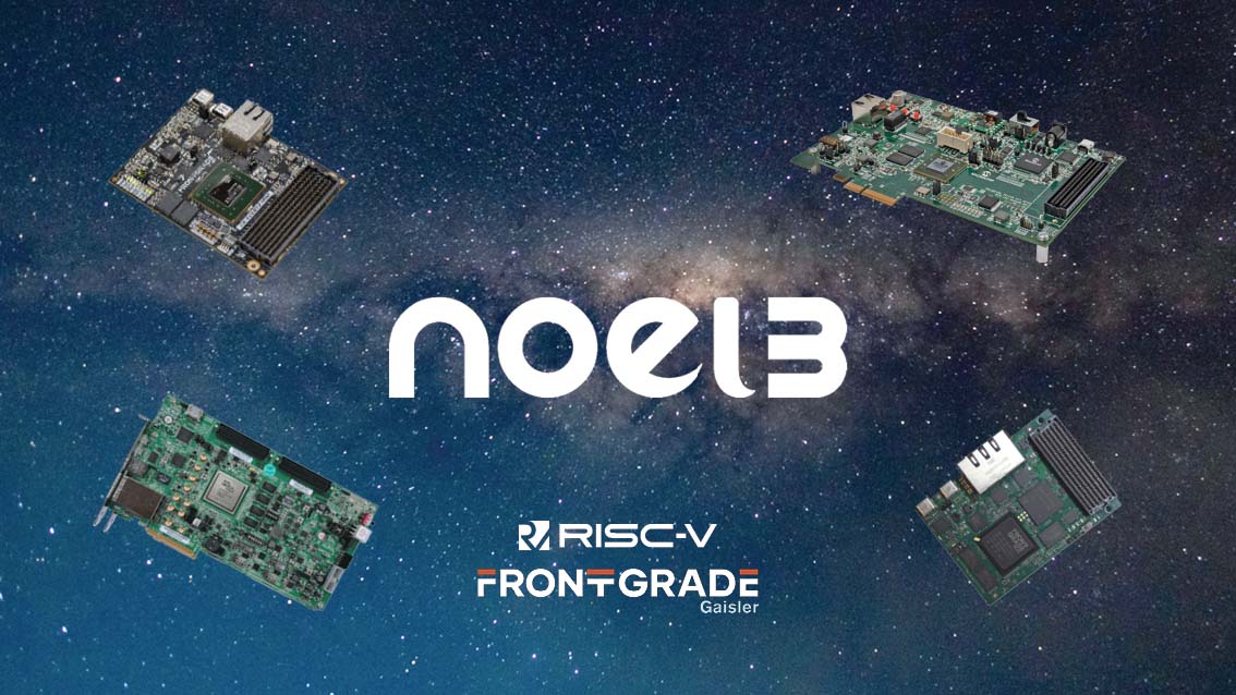
Full ecosystem for mission critical System-on-a-Chip solutions


.avif)
.avif)
.png)
.png)

-p-1600%20(1).avif)
.avif)

.avif)


.avif)
.avif)
.png)
.avif)
.avif)
.png)
.png)

.png)

.avif)

.avif)
.avif)
.avif)
.avif)


.avif)
.avif)
.avif)
.avif)
.avif)
.avif)
.avif)
.png)

.avif)
.avif)

.avif)
.avif)
.avif)
%20(1).avif)
%20(1).avif)
.avif)
.avif)
.avif)
.avif)
.avif)

.avif)

%20(1).avif)


.avif)


.avif)